Explain Ram Chip With Diagram
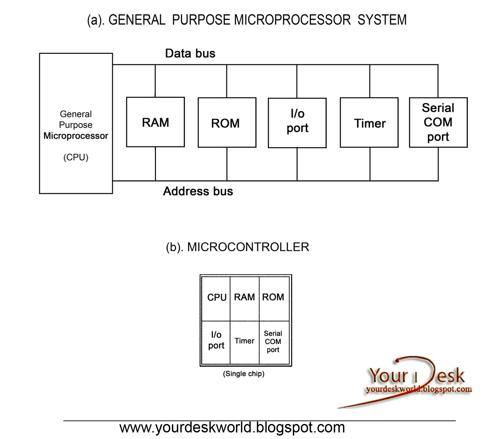
Microprocessor microcontroller diagram block cpu ram rom general purpose chip system contains io single counter Memory computer ram rom types different vs differences ddr tree between chart diagram difference explained why does so techyv hardware Main memory
RAM DESIGN Design a 8K x 8 RAM memory system, using 1 K x 8 memory
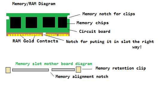
Ram diagram memory computer slot parts chip laptop pc access troubleshooting slots cpu contacts gold clean bad 2011 omg messed Inside intel's first product: the 3101 ram chip held just 64 bits What is ram (random access memory)?
Computer organization and architecture (memory organization)
Memory unit computer architectureRam block diagram Kcp316nd8/8Data random access memory (ram) — pyntel4004 env_version documentation.
Ram ddr3 operation representationDiagram ram rom sram block memory ic functional description Main memory8051 microcontroller kit circuit diagram.

Memory internal organization chip diagram interface address above shows
8051 memory organizationFunction of a ram in a computer : computer ram explained darren s study 8051 memory microcontroller organization ram hexadecimal data system special addresses eeprom external architecture addressing number purpose indirect mikroeComputer hardware: some useful parts of your pc.
Block diagram of microcontroller and microprocessorMémoire vive (ram) – part 2 – stacklima 20+ ram chip block diagramMemory organization internal chips computer architecture figure fig.

Rom 1k 256 chip decoder eight microchip input
Solved: using the 64k times 8 ram chip in figure 7-9 plusRom & ram: an introduction to computer memory Ram memory structure random access basic write ppt read powerpoint presentation select logic chip data lines addressRam and-rom-chips.
Explain ram chip with diagramMemory components ram ppt structure internal block presentation bit powerpoint storage cell Ram chip 64k diagram block using 1m computer question logic times plus figure fundamentals chapter book decoder construct solvedInternal organization of memory chips » examradar.
Internal chips examradar
Co and architecture: internal organization of memory chip.Computer organization Ram design design a 8k x 8 ram memory system, using 1 k x 8 memoryInternal organization of memory chips » examradar.
Chip typical rom upsc fever inputs gatecseChip ram inside diagram intel block bits held just first Memory explainedSolved design a 128k x 16 ram by using a block diagram of.

Electrical – construct an 32 x 8 ram using 4 of 16 x4 ram chips
Ram chip memory typical select random access write lines data read address ppt powerpoint presentationDekodierung der speichernomenklatur mit ram (arbeitsspeicher Random access memoryProjeto de 512 × 8 ram usando 128 × 8 ram – acervo lima.
.


Computer Organization | Internal organization of RAM chip - YouTube

Main Memory - Coding Ninjas

CO and Architecture: Internal organization of memory chip.

Solved: Using The 64K Times 8 RAM Chip In Figure 7-9 Plus | Chegg.com
COMPUTER HARDWARE: SOME USEFUL PARTS OF YOUR PC

Mémoire vive (RAM) – Part 2 – StackLima

RAM DESIGN Design a 8K x 8 RAM memory system, using 1 K x 8 memory